In a pivotal shift for the semiconductor industry, advanced packaging technologies are rapidly emerging as the new frontier for enhancing artificial intelligence (AI) chip capabilities and efficiency. As the traditional scaling limits of Moore's Law become increasingly apparent, these innovative packaging solutions are providing a critical pathway to overcome bottlenecks in performance, power consumption, and form factor, directly addressing the insatiable demands of modern AI workloads. This evolution is not merely about protecting chips; it's about fundamentally redesigning how components are integrated, enabling unprecedented levels of data throughput and computational density essential for the future of AI.
The immediate significance of this revolution is profound. AI applications, from large language models (LLMs) and computer vision to autonomous driving, require immense computational power, rapid data processing, and complex computations that traditional 2D chip designs can no longer adequately meet. Advanced packaging, by enabling tighter integration of diverse components like High Bandwidth Memory (HBM) and specialized processors, is directly tackling the "memory wall" bottleneck and facilitating the creation of highly customized, energy-efficient AI accelerators. This strategic pivot ensures that the semiconductor industry can continue to deliver the performance gains necessary to fuel the exponential growth of AI.
The Engineering Marvels Behind AI's Performance Leap
Advanced packaging techniques represent a significant departure from conventional chip manufacturing, moving beyond simply encapsulating a single silicon die. These innovations are designed to optimize interconnects, reduce latency, and integrate heterogeneous components into a unified, high-performance system.
One of the most prominent advancements is 2.5D Packaging, exemplified by technologies like TSMC's (Taiwan Semiconductor Manufacturing Company) CoWoS (Chip on Wafer on Substrate) and Intel's (a leading global semiconductor manufacturer) EMIB (Embedded Multi-die Interconnect Bridge). In 2.5D packaging, multiple dies – typically a logic processor and several stacks of High Bandwidth Memory (HBM) – are placed side-by-side on a silicon interposer. This interposer acts as a high-speed communication bridge, drastically reducing the distance data needs to travel compared to traditional printed circuit board (PCB) connections. This translates to significantly faster data transfer rates and higher bandwidth, often achieving interconnect speeds of up to 4.8 TB/s, a monumental leap from the less than 200 GB/s common in conventional systems. NVIDIA's (a leading designer of graphics processing units and AI hardware) H100 GPU, a cornerstone of current AI infrastructure, notably leverages a 2.5D CoWoS platform with HBM stacks and the GPU die on a silicon interposer, showcasing its effectiveness in real-world AI applications.
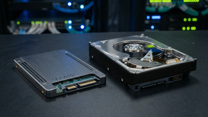
Building on this, 3D Packaging (3D-IC) takes integration to the next level by stacking multiple active dies vertically and connecting them with Through-Silicon Vias (TSVs). These tiny vertical electrical connections pass directly through the silicon dies, creating incredibly short interconnects. This offers the highest integration density, shortest signal paths, and unparalleled power efficiency, making it ideal for the most demanding AI accelerators and high-performance computing (HPC) systems. HBM itself is a prime example of 3D stacking, where multiple DRAM chips are stacked and interconnected to provide superior bandwidth and efficiency. This vertical integration not only boosts speed but also significantly reduces the overall footprint of the chip, meeting the demand for smaller, more portable devices and compact, high-density AI systems.
Further enhancing flexibility and scalability is Chiplet Technology. Instead of fabricating a single, large, monolithic chip, chiplets break down a processor into smaller, specialized components (e.g., CPU cores, GPU cores, AI accelerators, I/O controllers) that are then interconnected within a single package using advanced packaging systems. This modular approach allows for flexible design, improved performance, and better yield rates, as smaller dies are easier to manufacture defect-free. Major players like Intel, AMD (Advanced Micro Devices), and NVIDIA are increasingly adopting or exploring chiplet-based designs for their AI and data center GPUs, enabling them to customize solutions for specific AI tasks with greater agility and cost-effectiveness.
Beyond these, Fan-Out Wafer-Level Packaging (FOWLP) and Panel-Level Packaging (PLP) are also gaining traction. FOWLP extends the silicon die beyond its original boundaries, allowing for higher I/O density and improved thermal performance, often eliminating the need for a substrate. PLP, an even newer advancement, assembles and packages integrated circuits onto a single panel, offering higher density, lower manufacturing costs, and greater scalability compared to wafer-level packaging. Finally, Hybrid Bonding represents a cutting-edge technique, allowing for extremely fine interconnect pitches (single-digit micrometer range) and very high bandwidths by directly bonding dielectric and metal layers at the wafer level. This is crucial for achieving ultra-high-density integration in next-generation AI accelerators.
Initial reactions from the AI research community and industry experts have been overwhelmingly positive, viewing advanced packaging as a fundamental enabler for the next generation of AI. Experts like those at Applied Materials (a leading supplier of equipment for manufacturing semiconductors) have launched initiatives to accelerate the development and commercialization of these solutions, recognizing their critical role in sustaining the pace of AI innovation. The consensus is that these packaging innovations are no longer merely an afterthought but a core architectural component, radically reshaping the chip ecosystem and allowing AI to break through traditional computational barriers.
Reshaping the AI Industry: A New Competitive Landscape
The advent of advanced semiconductor packaging is fundamentally reshaping the competitive landscape across the AI industry, creating new opportunities and challenges for tech giants, specialized AI companies, and nimble startups alike. This technological shift is no longer a peripheral concern but a central pillar of strategic differentiation and market dominance in the era of increasingly sophisticated AI.
Tech giants are at the forefront of this transformation, recognizing advanced packaging as indispensable for their AI ambitions. Companies like Google (a global technology leader), Meta (the parent company of Facebook, Instagram, and WhatsApp), Amazon (a multinational technology company), and Microsoft (a leading multinational technology corporation) are making massive investments in AI and data center expansion, with Amazon alone earmarking $100 billion for AI and data center expansion in 2025. These investments are intrinsically linked to the development and deployment of advanced AI chips that leverage these packaging solutions. Their in-house AI chip development efforts, such as Google's Tensor Processing Units (TPUs) and Amazon's Inferentia and Trainium chips, heavily rely on these innovations to achieve the necessary performance and efficiency.
The most direct beneficiaries are the foundries and Integrated Device Manufacturers (IDMs) that possess the advanced manufacturing capabilities. TSMC (Taiwan Semiconductor Manufacturing Company), with its cutting-edge CoWoS and SoIC technologies, has become an indispensable partner for nearly all leading AI chip designers, including NVIDIA and AMD. Intel (a leading global semiconductor manufacturer) is aggressively investing in its own advanced packaging capabilities, such as EMIB, and building new fabs to strengthen its position as both a designer and manufacturer. Samsung (a South Korean multinational manufacturing conglomerate) is also a key player, developing its own 3.3D advanced packaging technology to offer competitive solutions.
Fabless chipmakers and AI chip designers are leveraging advanced packaging to deliver their groundbreaking products. NVIDIA (a leading designer of graphics processing units and AI hardware), with its H100 AI chip utilizing TSMC's CoWoS packaging, exemplifies the immediate performance gains. AMD (Advanced Micro Devices) is following suit with its MI300 series, while Broadcom (a global infrastructure technology company) is developing its 3.5D XDSiP platform for networking solutions critical to AI data centers. Even Apple (a multinational technology company known for its consumer electronics), with its M2 Ultra chip, showcases the power of advanced packaging to integrate multiple dies into a single, high-performance package for its high-end computing needs.
The shift also creates significant opportunities for Outsourced Semiconductor Assembly and Test (OSAT) Vendors like ASE Technology Holding, which are expanding their advanced packaging offerings and developing chiplet interconnect technologies. Similarly, Semiconductor Equipment Manufacturers such as Applied Materials (a leading supplier of equipment for manufacturing semiconductors), KLA (a capital equipment company), and Lam Research (a global supplier of wafer fabrication equipment) are positioned to benefit immensely, providing the essential tools and solutions for these complex manufacturing processes. Electronic Design Automation (EDA) Software Vendors like Synopsys (a leading electronic design automation company) are also crucial, as AI itself is poised to transform the entire EDA flow, automating IC layout and optimizing chip production.
Competitively, advanced packaging is transforming the semiconductor value chain. Value creation is increasingly migrating towards companies capable of designing and integrating complex, system-level chip solutions, elevating the strategic importance of back-end design and packaging. This differentiation means that packaging is no longer a commoditized process but a strategic advantage. Companies that integrate advanced packaging into their offerings are gaining a significant edge, while those clinging to traditional methods risk being left behind. The intricate nature of these packages also necessitates intense collaboration across the industry, fostering new partnerships between chip designers, foundries, and OSATs. Business models are evolving, with foundries potentially seeing reduced demand for large monolithic SoCs as multi-chip packages become more prevalent. Geopolitical factors, such as the U.S. CHIPS Act and Europe's Chips Act, further influence this landscape by providing substantial incentives for domestic advanced packaging capabilities, shaping supply chains and market access.
The disruption extends to design philosophy itself, moving beyond Moore's Law by focusing on combining smaller, optimized chiplets rather than merely shrinking transistors. This "More than Moore" approach, enabled by advanced packaging, improves performance, accelerates time-to-market, and reduces manufacturing costs and power consumption. While promising, these advanced processes are more energy-intensive, raising concerns about the environmental impact, a challenge that chiplet technology aims to mitigate partly through improved yields. Companies are strategically positioning themselves by focusing on system-level solutions, making significant investments in packaging R&D, and specializing in innovative techniques like hybrid bonding. This strategic positioning, coupled with global expansion and partnerships, is defining who will lead the AI hardware race.
A Foundational Shift in the Broader AI Landscape
Advanced semiconductor packaging represents a foundational shift that is profoundly impacting the broader AI landscape and its prevailing trends. It is not merely an incremental improvement but a critical enabler, pushing the boundaries of what AI systems can achieve as traditional monolithic chip design approaches increasingly encounter physical and economic limitations. This strategic evolution allows AI to continue its exponential growth trajectory, unhindered by the constraints of a purely 2D scaling paradigm.
This packaging revolution is intrinsically linked to the rise of Generative AI and Large Language Models (LLMs). These sophisticated models demand unprecedented processing power and, crucially, high-bandwidth memory. Advanced packaging, through its ability to integrate memory and processors in extremely close proximity, directly addresses this need, providing the high-speed data transfer pathways essential for training and deploying such computationally intensive AI. Similarly, the drive towards Edge AI and Miniaturization for applications in mobile devices, IoT, and autonomous vehicles is heavily reliant on advanced packaging, which enables the creation of smaller, more powerful, and energy-efficient devices. The principle of Heterogeneous Integration, allowing for for the combination of diverse chip types—CPUs, GPUs, specialized AI accelerators, and memory—within a single package, optimizes computing power for specific tasks and creates more versatile, bespoke AI solutions for an increasingly diverse set of applications. For High-Performance Computing (HPC), advanced packaging is indispensable, facilitating the development of supercomputers capable of handling the massive processing requirements of AI by enabling customization of memory, processing power, and other resources.
The impacts of advanced packaging on AI are multifaceted and transformative. It delivers optimized performance by significantly reducing data transfer distances, leading to faster processing, lower latency, and higher bandwidth—critical for AI workloads like model training and deep learning inference. NVIDIA's H100 GPU, for example, leverages 2.5D packaging to integrate HBM with its central IC, achieving bandwidths previously thought impossible. Concurrently, enhanced energy efficiency is achieved through shorter interconnect paths, which reduce energy dissipation and minimize power loss, a vital consideration given the substantial power consumption of large AI models. While initially complex, cost efficiency is also a long-term benefit, particularly through chiplet technology. By allowing manufacturers to use smaller, defect-free chiplets and combine them, it reduces manufacturing losses and overall costs compared to producing large, monolithic chips, enabling the use of cost-optimal manufacturing technology for each chiplet. Furthermore, scalability and flexibility are dramatically improved, as chiplets offer modularity that allows for customizability and the integration of additional components without full system overhauls. Finally, the ability to stack components vertically facilitates miniaturization, meeting the growing demand for compact and portable AI devices.
Despite these immense benefits, several potential concerns accompany the widespread adoption of advanced packaging. The inherent manufacturing complexity and cost of processes like 3D stacking and Through-Silicon Via (TSV) integration require significant investment, specialized equipment, and expertise. Thermal management presents another major challenge, as densely packed, high-performance AI chips generate substantial heat, necessitating advanced cooling solutions. Supply chain constraints are also a pressing issue, with demand for state-of-art facilities and expertise for advanced packaging rapidly outpacing supply, leading to production bottlenecks and geopolitical tensions, as evidenced by export controls on advanced AI chips. The environmental impact of more energy-intensive and resource-demanding manufacturing processes is a growing concern. Lastly, ensuring interoperability and standardization between chiplets from different manufacturers is crucial, with initiatives like the Universal Chiplet Interconnect Express (UCIe) Consortium working to establish common standards.
Comparing advanced packaging to previous AI milestones reveals its profound significance. For decades, AI progress was largely fueled by Moore's Law and the ability to shrink transistors. As these limits are approached, advanced packaging, especially the chiplet approach, offers an alternative pathway to performance gains through "more than Moore" scaling and heterogeneous integration. This is akin to the shift from simply making transistors smaller to finding new architectural ways to combine and optimize computational elements, fundamentally redefining how performance is achieved. Just as the development of powerful GPUs (e.g., NVIDIA's CUDA) enabled the deep learning revolution by providing parallel processing capabilities, advanced packaging is enabling the current surge in generative AI and large language models by addressing the data transfer bottleneck. This marks a shift towards system-level innovation, where the integration and interconnection of components are as critical as the components themselves, a holistic approach to chip design that NVIDIA CEO Jensen Huang has highlighted as equally crucial as chip design advancements. While early AI hardware was often custom and expensive, advanced packaging, through cost-effective chiplet design and panel-level manufacturing, has the potential to make high-performance AI processors more affordable and accessible, paralleling how commodity hardware and open-source software democratized early AI research. In essence, advanced packaging is not just an improvement; it is a foundational technology underpinning the current and future advancements in AI.
The Horizon of AI: Future Developments in Advanced Packaging
The trajectory of advanced semiconductor packaging for AI chips is one of continuous innovation and expansion, promising to unlock even more sophisticated and pervasive artificial intelligence capabilities in the near and long term. As the demands of AI continue to escalate, these packaging technologies will remain at the forefront of hardware evolution, shaping the very architecture of future computing.
In the near-term (next 1-5 years), we can expect a widespread adoption and refinement of existing advanced packaging techniques. 2.5D and 3D hybrid bonding will become even more critical for optimizing system performance in AI and High-Performance Computing (HPC), with companies like TSMC (Taiwan Semiconductor Manufacturing Company) and Intel (a leading global semiconductor manufacturer) continuing to push the boundaries of their CoWoS and EMIB technologies, respectively. Chiplet architectures will gain significant traction, becoming the standard for complex AI systems due to their modularity, improved yield, and cost-effectiveness. Innovations in Fan-Out Wafer-Level Packaging (FOWLP) and Fan-Out Panel-Level Packaging (FOPLP) will offer more cost-effective and higher-performance solutions for increased I/O density and thermal dissipation, especially for AI chips in consumer electronics. The emergence of glass substrates as a promising alternative will offer superior dimensional stability and thermal properties for demanding applications like automotive and high-end AI. Crucially, Co-Packaged Optics (CPO), integrating optical communication directly into the package, will gain momentum to address the "memory wall" challenge, offering significantly higher bandwidth and lower transmission loss for data-intensive AI. Furthermore, Heterogeneous Integration will become a key enabler, combining diverse components with different functionalities into highly optimized AI systems, while AI-driven design automation will leverage AI itself to expedite chip production by automating IC layout and optimizing power, performance, and area (PPA).
Looking further into the long-term (5+ years), advanced packaging is poised to redefine the semiconductor industry fundamentally. AI's proliferation will extend significantly beyond large data centers into "Edge AI" and dedicated AI devices, impacting PCs, smartphones, and a vast array of IoT devices, necessitating highly optimized, low-power, and high-performance packaging solutions. The market will likely see the emergence of new packaging technologies and application-specific integrated circuits (ASICs) tailored for increasingly specialized AI tasks. Advanced packaging will also play a pivotal role in the scalability and reliability of future computing paradigms such as quantum processors (requiring unique materials and designs) and neuromorphic chips (focusing on ultra-low power consumption and improved connectivity to mimic the human brain). As Moore's Law faces fundamental physical and economic limitations, advanced packaging will firmly establish itself as the primary driver for performance improvements, becoming the "new king" of innovation, akin to the transistor in previous eras.
The potential applications and use cases are vast and transformative. Advanced packaging is indispensable for Generative AI (GenAI) and Large Language Models (LLMs), providing the immense computational power and high memory bandwidth required. It underpins High-Performance Computing (HPC) for data centers and supercomputers, ensuring the necessary data throughput and energy efficiency. In mobile devices and consumer electronics, it enables powerful AI capabilities in compact form factors through miniaturization and increased functionality. Automotive computing for Advanced Driver-Assistance Systems (ADAS) and autonomous driving heavily relies on complex, high-performance, and reliable AI chips facilitated by advanced packaging. The deployment of 5G and network infrastructure also necessitates compact, high-performance devices capable of handling massive data volumes at high speeds, driven by these innovations. Even small medical equipment like hearing aids and pacemakers are integrating AI functionalities, made possible by the miniaturization benefits of advanced packaging.
However, several challenges need to be addressed for these future developments to fully materialize. The manufacturing complexity and cost of advanced packages, particularly those involving interposers and Through-Silicon Vias (TSVs), require significant investment and robust quality control to manage yield challenges. Thermal management remains a critical hurdle, as increasing power density in densely packed AI chips necessitates continuous innovation in cooling solutions. Supply chain management becomes more intricate with multichip packaging, demanding seamless orchestration across various designers, foundries, and material suppliers, which can lead to constraints. The environmental impact of more energy-intensive and resource-demanding manufacturing processes requires a greater focus on "Design for Sustainability" principles. Design and validation complexity for EDA software must evolve to simulate the intricate interplay of multiple chips, including thermal dissipation and warpage. Finally, despite advancements, the persistent memory bandwidth limitations (memory wall) continue to drive the need for innovative packaging solutions to move data more efficiently.
Expert predictions underscore the profound and sustained impact of advanced packaging on the semiconductor industry. The advanced packaging market is projected to grow substantially, with some estimates suggesting it will double by 2030 to over $96 billion, significantly outpacing the rest of the chip industry. AI applications are expected to be a major growth driver, potentially accounting for 25% of the total advanced packaging market and growing at approximately 20% per year through the next decade, with the market for advanced packaging in AI chips specifically projected to reach around $75 billion by 2033. The overall semiconductor market, fueled by AI, is on track to reach about $697 billion in 2025 and aims for the $1 trillion mark by 2030. Advanced packaging, particularly 2.5D and 3D heterogeneous integration, is widely seen as the "key enabler of the next microelectronic revolution," becoming as fundamental as the transistor was in the era of Moore's Law. This will elevate the role of system design and shift the focus within the semiconductor value chain, with back-end design and packaging gaining significant importance and profit value alongside front-end manufacturing. Major players like TSMC, Samsung, and Intel are heavily investing in R&D and expanding their advanced packaging capabilities to meet this surging demand from the AI sector, solidifying its role as the backbone of future AI innovation.
The Unseen Revolution: A Wrap-Up
The journey of advanced packaging from a mere protective shell to a core architectural component marks an unseen revolution fundamentally transforming the landscape of AI hardware. The key takeaways are clear: advanced packaging is indispensable for performance enhancement, enabling unprecedented data exchange speeds crucial for AI workloads like LLMs; it drives power efficiency by optimizing interconnects, making high-performance AI economically viable; it facilitates miniaturization for compact and powerful AI devices across various sectors; and through chiplet architectures, it offers avenues for cost reduction and faster time-to-market. Furthermore, its role in heterogeneous integration is pivotal for creating versatile and adaptable AI solutions. The market reflects this, with advanced packaging projected for substantial growth, heavily driven by AI applications.
In the annals of AI history, advanced packaging's significance is akin to the invention of the transistor or the advent of the GPU. It has emerged as a critical enabler, effectively overcoming the looming limitations of Moore's Law by providing an alternative path to higher performance through multi-chip integration rather than solely transistor scaling. Its role in enabling High-Bandwidth Memory (HBM), crucial for the data-intensive demands of modern AI, cannot be overstated. By addressing these fundamental hardware bottlenecks, advanced packaging directly drives AI innovation, fueling the rapid advancements we see in generative AI, autonomous systems, and edge computing.
The long-term impact will be profound. Advanced packaging will remain critical for continued AI scalability, solidifying chiplet-based designs as the new standard for complex systems. It will redefine the semiconductor ecosystem, elevating the importance of system design and the "back end" of chipmaking, necessitating closer collaboration across the entire value chain. While sustainability challenges related to energy and resource intensity remain, the industry's focus on eco-friendly materials and processes, coupled with the potential of chiplets to improve overall production efficiency, will be crucial. We will also witness the emergence of new technologies like co-packaged optics and glass-core substrates, further revolutionizing data transfer and power efficiency. Ultimately, by making high-performance AI chips more cost-effective and energy-efficient, advanced packaging will facilitate the broader adoption of AI across virtually every industry.
In the coming weeks and months, what to watch for includes the progression of next-generation packaging solutions like FOPLP, glass-core substrates, 3.5D integration, and co-packaged optics. Keep an eye on major player investments and announcements from giants like TSMC, Samsung, Intel, AMD, NVIDIA, and Applied Materials, as their R&D efforts and capacity expansions will dictate the pace of innovation. Observe the increasing heterogeneous integration adoption rates across AI and HPC segments, evident in new product launches. Monitor the progress of chiplet standards and ecosystem development, which will be vital for fostering an open and flexible chiplet environment. Finally, look for a growing sustainability focus within the industry, as it grapples with the environmental footprint of these advanced processes.
This content is intended for informational purposes only and represents analysis of current AI developments.
TokenRing AI delivers enterprise-grade solutions for multi-agent AI workflow orchestration, AI-powered development tools, and seamless remote collaboration platforms.
For more information, visit https://www.tokenring.ai/.