As of January 1, 2026, the global semiconductor landscape is defined by a singular, high-stakes conflict: the "HBM War." High-bandwidth memory (HBM) has transitioned from a specialized component to the most critical bottleneck in the artificial intelligence supply chain. With the demand for generative AI models continuing to outpace hardware availability, the rivalry between the two South Korean titans, SK Hynix (KRX: 000660) and Samsung Electronics (KRX: 005930), has reached a fever pitch. While SK Hynix enters 2026 holding the crown of market leader, Samsung is leveraging its massive industrial scale to mount a comeback that could reshape the future of AI silicon.
The immediate significance of this development cannot be overstated. The industry is currently transitioning from the mature HBM3E standard, which powers the current generation of AI accelerators, to the paradigm-shifting HBM4 architecture. This next generation of memory is not merely an incremental speed boost; it represents a fundamental change in how computers are built. By moving toward 3D stacking and placing memory directly onto logic chips, the industry is attempting to shatter the "memory wall"—the physical limit on how fast data can move between a processor and its memory—which has long been the primary constraint on AI performance.
The Technical Leap: 2048-bit Interfaces and the 3D Stacking Revolution
The technical specifications of the upcoming HBM4 modules, slated for mass production in February 2026, represent a gargantuan leap over the HBM3E standard that dominated 2024 and 2025. HBM4 doubles the memory interface width from 1024-bit to 2048-bit, enabling bandwidth speeds exceeding 2.0 to 2.8 terabytes per second (TB/s) per stack. This massive throughput is essential for the 100-trillion parameter models expected to emerge later this year, which require near-instantaneous access to vast datasets to maintain low latency in real-time applications.
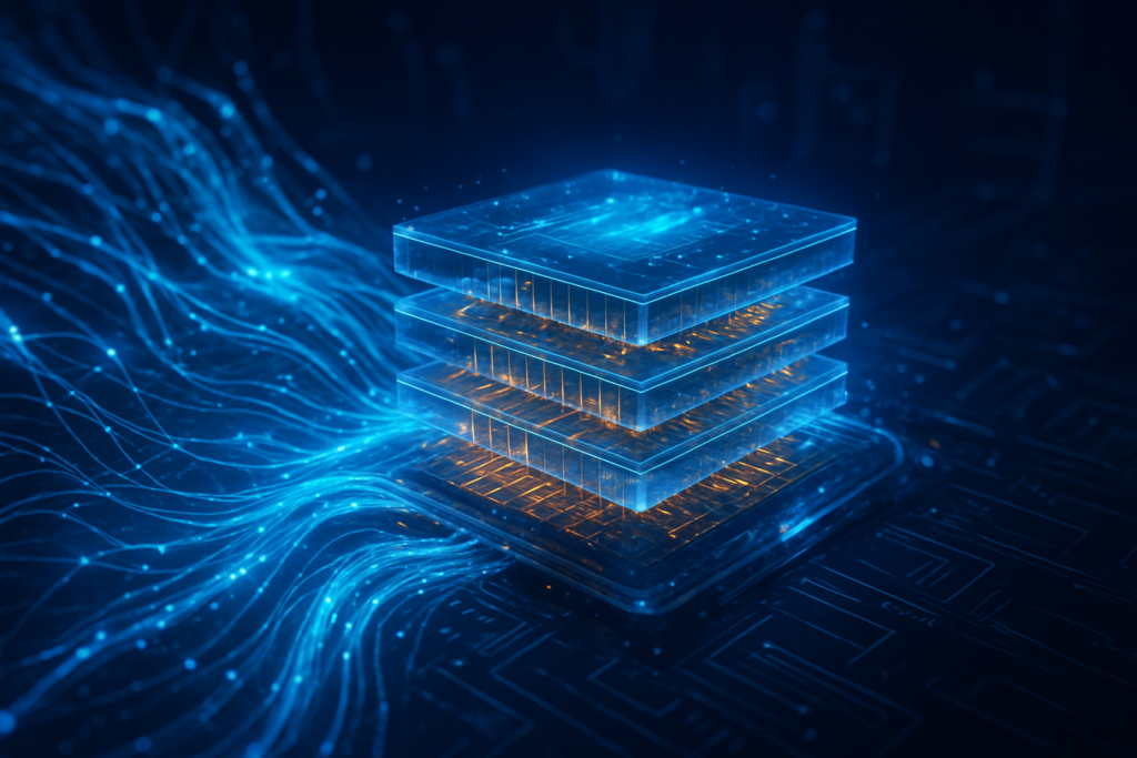
Perhaps the most significant architectural change is the evolution of the "Base Die"—the bottom layer of the HBM stack. In previous generations, this die was manufactured using standard memory processes. With HBM4, the base die is being shifted to high-performance logic processes, such as 5nm or 4nm nodes. This allows for the integration of custom logic directly into the memory stack, effectively blurring the line between memory and processor. SK Hynix has achieved this through a landmark "One-Team" alliance with TSMC (NYSE: TSM), using the latter's world-class foundry capabilities to manufacture the base die. In contrast, Samsung is utilizing its "All-in-One" strategy, handling everything from DRAM production to logic die fabrication and advanced packaging within its own ecosystem.
The manufacturing methods have also diverged into two competing philosophies. SK Hynix continues to refine its Advanced MR-MUF (Mass Reflow Molded Underfill) process, which has proven superior in thermal dissipation and yield stability for 12-layer stacks. Samsung, however, is aggressively pivoting to Hybrid Bonding (copper-to-copper direct bonding) for its 16-layer HBM4 samples. By eliminating the micro-bumps traditionally used to connect layers, Hybrid Bonding significantly reduces the height of the stack and improves electrical efficiency. Initial reactions from the AI research community suggest that while MR-MUF is the reliable choice for today, Hybrid Bonding may be the inevitable winner as stacks grow to 20 layers and beyond.
Market Positioning: The Race to Supply the "Rubin" Era
The primary arbiter of this war remains NVIDIA (NASDAQ: NVDA). As of early 2026, SK Hynix maintains a dominant market share of approximately 57% to 60%, largely due to its status as the primary supplier for NVIDIA’s Blackwell and Blackwell Ultra platforms. However, the upcoming NVIDIA "Rubin" (R100) platform, designed specifically for HBM4, has created a clean slate for competition. Each Rubin GPU is expected to utilize eight HBM4 stacks, making the procurement of these chips the single most important strategic goal for cloud service providers like Microsoft (NASDAQ: MSFT) and Google (NASDAQ: GOOGL).
Samsung, which held roughly 22% to 30% of the market at the end of 2025, is betting on its "turnkey" advantage to reclaim the lead. By offering a one-stop-shop service—where memory, logic, and packaging are handled under one roof—Samsung claims it can reduce supply chain timelines by up to 20% compared to the SK Hynix and TSMC partnership. This vertical integration is a powerful lure for AI labs looking to secure guaranteed volume in a market where shortages are still common. Meanwhile, Micron Technology (NASDAQ: MU) remains a formidable third player, capturing nearly 20% of the market by focusing on high-efficiency HBM3E for specialized AMD (NASDAQ: AMD) and custom hyperscaler chips.
The competitive implications are stark: if Samsung can successfully qualify its 16-layer HBM4 with NVIDIA before SK Hynix, it could trigger a massive shift in market share. Conversely, if the SK Hynix-TSMC alliance continues to deliver superior yields, Samsung may find itself relegated to a secondary supplier role for another generation. For AI startups and major labs, this competition is a double-edged sword; while it drives innovation and theoretically lowers prices, the divergence in technical standards (MR-MUF vs. Hybrid Bonding) adds complexity to hardware design and procurement strategies.
Shattering the Memory Wall: Wider Significance for the AI Landscape
The shift toward HBM4 and 3D stacking fits into a broader trend of "domain-specific" computing. For decades, the industry followed the von Neumann architecture, where memory and processing are separate. The HBM4 era marks the beginning of the end for this paradigm. By placing memory directly on logic chips, the industry is moving toward a "near-memory computing" model. This is crucial for power efficiency; in modern AI workloads, moving data between the chip and the memory often consumes more energy than the actual calculation itself.
This development also addresses a growing concern among environmental and economic observers: the staggering power consumption of AI data centers. HBM4’s increased efficiency per gigabyte of bandwidth is a necessary evolution to keep the growth of AI sustainable. However, the transition is not without risks. The complexity of 3D stacking and Hybrid Bonding increases the potential for catastrophic yield failures, which could lead to sudden price spikes or supply chain disruptions. Furthermore, the deepening alliance between SK Hynix and TSMC centralizes a significant portion of the AI hardware ecosystem in a few key partnerships, raising concerns about market concentration.
Compared to previous milestones, such as the transition from DDR4 to DDR5, the HBM3E-to-HBM4 shift is far more disruptive. It is not just a component upgrade; it is a re-engineering of the semiconductor stack. This transition mirrors the early days of the smartphone revolution, where the integration of various components into a single System-on-Chip (SoC) led to a massive explosion in capability and efficiency.
Looking Ahead: HBM4E and the Custom Memory Era
In the near term, the industry is watching for the first "Production Readiness Approval" (PRA) for HBM4-equipped GPUs. Experts predict that the first half of 2026 will be defined by a "war of nerves" as Samsung and SK Hynix race to meet NVIDIA’s stringent quality standards. Beyond HBM4, the roadmap already points toward HBM4E, which is expected to push 3D stacking to 20 layers and introduce even more complex logic integration, potentially allowing for AI inference tasks to be performed entirely within the memory stack itself.
One of the most anticipated future developments is the rise of "Custom HBM." Instead of buying off-the-shelf memory modules, tech giants like Amazon (NASDAQ: AMZN) and Meta (NASDAQ: META) are beginning to request bespoke HBM designs tailored to their specific AI silicon. This would allow for even tighter integration and better performance for specific workloads, such as large language model (LLM) training or recommendation engines. The challenge for memory makers will be balancing the high volume required by NVIDIA with the specialized needs of these custom-chip customers.
Conclusion: A New Chapter in Semiconductor History
The HBM war between SK Hynix and Samsung represents a defining moment in the history of artificial intelligence. As we move into 2026, the successful deployment of HBM4 will determine which companies lead the next decade of AI innovation. SK Hynix’s current dominance, built on engineering precision and a strategic alliance with TSMC, is being tested by Samsung’s massive vertical integration and its bold leap into Hybrid Bonding.
The key takeaway for the industry is that memory is no longer a commodity; it is a strategic asset. The ability to stack 16 layers of DRAM onto a logic die with micrometer precision is now as important to the future of AI as the algorithms themselves. In the coming weeks and months, the industry will be watching for yield reports and qualification announcements that will signal who has the upper hand in the Rubin era. For now, the "memory wall" is being dismantled, layer by layer, in the cleanrooms of South Korea and Taiwan.
This content is intended for informational purposes only and represents analysis of current AI developments.
TokenRing AI delivers enterprise-grade solutions for multi-agent AI workflow orchestration, AI-powered development tools, and seamless remote collaboration platforms.
For more information, visit https://www.tokenring.ai/.