The foundation of artificial intelligence is no longer just code and silicon; it is increasingly becoming glass. As of January 2026, the semiconductor industry has reached a pivotal turning point, officially transitioning away from traditional organic substrates like Ajinomoto Build-up Film (ABF) in favor of glass substrates. This shift, led by pioneers like Intel (NASDAQ: INTC) and SKC (KRX: 011790) through its subsidiary Absolics, marks the end of the "warpage wall" that has plagued high-heat AI chips for years.
The immediate significance of this transition cannot be overstated. As AI accelerators from NVIDIA (NASDAQ: NVDA) and AMD (NASDAQ: AMD) push toward and beyond the 1,000-watt power envelope, traditional organic materials have proven too flexible and thermally unstable to support the massive, multi-die "super-chips" required for generative AI. Glass substrates provide the structural integrity and thermal precision necessary to pack trillions of transistors and dozens of High Bandwidth Memory (HBM) stacks into a single, cohesive package, effectively setting the stage for the next decade of AI hardware scaling.
The Technical Edge: Solving the Warpage Wall
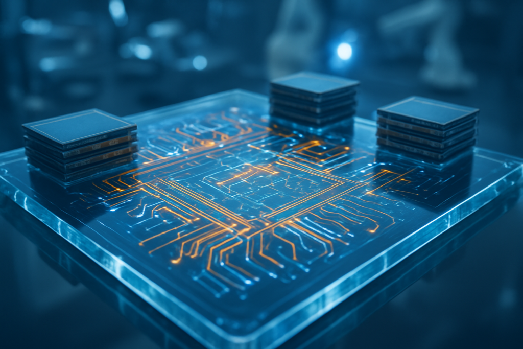
The move to glass is driven by fundamental physics. Traditional organic substrates are essentially high-tech plastics that expand and contract at different rates than the silicon chips they support. This "Coefficient of Thermal Expansion" (CTE) mismatch causes chips to warp as they heat up, leading to cracked micro-bumps and signal failure. Glass, however, has a CTE that closely matches silicon (3–5 ppm/°C), ensuring that even under the extreme 100°C+ temperatures of an AI data center, the substrate remains perfectly flat.
Technically, glass offers a level of precision that organic materials cannot match. While ABF-based substrates rely on mechanical drilling for "vias" (the vertical connections between layers), glass utilizes laser-etched Through-Glass Vias (TGV). This allows for an interconnect density nearly ten times higher than previous technologies, with pitches shrinking from 100μm to less than 10μm. Furthermore, glass boasts sub-1nm surface roughness, providing an ultra-flat canvas that improves lithography focus and allows for the etching of much finer circuits.
This transition also addresses power efficiency. Glass has approximately 50% lower dielectric loss than organic materials, meaning less energy is wasted as heat when data moves between the GPU and its memory. For the research community, this means AI models can be trained on hardware that is not only faster but significantly more energy-efficient, a critical factor as global data center power consumption continues to skyrocket in 2026.
Market Positioning: Intel, SKC, and the Battle for Packaging Supremacy
Intel has positioned itself as the clear leader in this space, having invested over $1 billion in its commercial-grade glass substrate pilot line in Chandler, Arizona. By January 2026, this facility is actively producing glass cores for Intel’s 18A and 14A process nodes. Intel’s strategy is one of vertical integration; by controlling the substrate production in-house, Intel Foundry aims to attract "hyperscalers" like Google and Microsoft who are designing custom AI silicon and require the highest possible yields for their massive chip designs.
Meanwhile, SKC’s subsidiary, Absolics—backed by Applied Materials (NASDAQ: AMAT)—has become the primary merchant supplier for the rest of the industry. Their $600 million facility in Covington, Georgia, reached a major milestone in late 2025 and is now ramping up to produce 20,000 sheets per month. Absolics has already secured high-profile partnerships with AMD and Amazon Web Services (AWS). For AMD, the use of Absolics' glass substrates in its Instinct MI400 series provides a strategic advantage, allowing them to offer higher memory bandwidth and better thermal management than competitors still reliant on older packaging techniques.
Samsung (KRX: 005930) has also entered the fray with its "Triple Alliance" strategy, coordinating between its electronics, display, and electro-mechanics divisions. At CES 2026, Samsung announced that its high-volume pilot line in Sejong, South Korea, is ready for mass production by the end of the year. This competitive pressure is forcing a rapid evolution in the supply chain, as even TSMC (NYSE: TSM) has begun sampling glass-based panels to ensure it can support NVIDIA’s upcoming "Rubin" R100 GPUs, which are expected to be the first major consumer of glass-integrated packaging at scale.
A Broader Shift in the AI Landscape
The adoption of glass substrates fits into a broader trend toward "Panel-Level Packaging" (PLP). For decades, chips were packaged on circular silicon wafers. Glass allows for large, rectangular panels that can fit significantly more chips per batch, dramatically increasing manufacturing throughput. This transition is reminiscent of the industry’s move from 200mm to 300mm wafers, but with even greater implications for the physical size of AI processors.
However, this shift is not without concerns. The transition to glass requires a complete overhaul of the back-end assembly process. Glass is brittle, and handling large, thin sheets of it in a high-speed manufacturing environment presents significant breakage risks. Industry experts have compared this milestone to the introduction of Extreme Ultraviolet (EUV) lithography—a necessary but painful transition that separates the leaders from the laggards in the semiconductor race.
Furthermore, the move to glass is a key enabler for HBM4, the next generation of high-bandwidth memory. As memory stacks grow taller and more numerous, the substrate must be strong enough to support the weight and heat of 12 or 16 HBM cubes surrounding a central processor. Without glass, the "super-chips" envisioned for the 2027–2030 era would simply be impossible to manufacture with reliable yields.
Future Horizons: Co-Packaged Optics and Beyond
Looking ahead, the roadmap for glass substrates extends far beyond simple structural support. By 2027, experts predict the integration of Co-Packaged Optics (CPO) directly onto glass substrates. Because glass is transparent and can be manufactured with high optical clarity, it is the ideal medium for routing light signals (photons) instead of electrical signals (electrons) between chips. This would effectively eliminate the "memory wall," allowing for near-instantaneous communication between GPUs in a massive AI cluster.
The near-term challenge remains yield optimization. While Intel and Absolics have proven the technology in pilot lines, scaling to millions of units per month will require further refinements in laser-drilling speed and glass-handling robotics. As we move into the latter half of 2026, the industry will be watching closely to see if glass-packaged chips can maintain their performance advantages without a significant increase in manufacturing costs.
Conclusion: The New Standard for AI
The shift to glass substrates represents one of the most significant architectural changes in semiconductor packaging history. By solving the dual challenges of flatness and thermal stability, Intel, SKC, and Samsung have provided the industry with a new foundation upon which the next generation of AI can be built. The "warpage wall" has been dismantled, replaced by a transparent, ultra-flat medium that enables the 1,000-watt processors of tomorrow.
As we move through 2026, the primary metric for success will be how quickly these companies can scale production to meet the insatiable demand for AI compute. With NVIDIA’s Rubin architecture and AMD’s MI400 series on the horizon, the "Glass Revolution" is no longer a future prospect—it is the current reality of the AI hardware market. Investors and tech enthusiasts should watch for the first third-party benchmarks of these glass-packaged chips in the coming months, as they will likely set new records for both performance and efficiency.
This content is intended for informational purposes only and represents analysis of current AI developments.
TokenRing AI delivers enterprise-grade solutions for multi-agent AI workflow orchestration, AI-powered development tools, and seamless remote collaboration platforms.
For more information, visit https://www.tokenring.ai/.